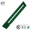
- Double-Sided PCB[10]
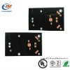
- Multilayer PCB[10]
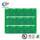
- Other PCB & PCBA[10]
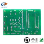
- Rigid PCB[10]
- Contact Person : Ms. Ma Sunny
- Company Name : Shenzhen Hongmy Precision Circuit Co., Ltd.
- Tel : 86-755-26954084-606
- Fax : 86-755-86372653
- Address : Guangdong,Shenzhen,B4-5 building,yanchuan north industial park, Songgang Town, Bao'an District, Shenzhen
- Country/Region : China
- Zip : 518105
FR-4 single side 1 layer pcb bare board


Related Product Searches:FR-4 single side 1 layer pcb bare board,High Quality,1 layer pcb, single side pcb,HM-Z050
pcb
PRODUCTION CAPABILITY
Layers: 1-20 layers
Material: FR-4, Aluminium Base, Rogers, Taconic, Teflon
Finish Board Thickness: 0.2mm-3.2mm (8mil-126mil)
External Copper Thickness: 35um-210um (1OZ-6OZ)
Internal Copper Thickness: 17um-140um(1/2OZ-4OZ)
Copper Plating Hole: 18um-40um
Min. Trace Width& Line Spacing: 0.075mm/ 0.1mm (3mil/4mil)
Min. Hole Dimension (CNC): 0.20mm (8mil)
Min. Hole Dimension (Punching): 0.9mm (35mil)
Max. Panel Dimension: 610mm x 508mm
Hole Position Tolerance CNC): +/-0.075mm (3mil)
Hole Dimension Tolerance (CNC): PTH : +/-0.075mm (3mil) NPTH :+/-0.05mm (2mil)
Outline Tolerance: CNC: +/-0.125mm (5mil) Punching: +/-0.15mm (6mil)
Warp& Twist: 0.70%
Min. Solder Mask Bridge: 0.0635mm (2.5mil)
Distance Between Line To Board Bridge: Outline: 0.25mm V-CUT: 0.40mm
Impedance Control Tolerance: +/-10%
Test Voltage: 10-300V
Solder Mask Types: Green, White, Blue, Red, Matt Green, Matt Black etc.
Surface Finishing: Lead Free Hot Air Leveling (HASL), HAL;
Immersion Gold (ENLG), Immersion Silver, Immersion Tin;
Electronic Gold (Plate Gold), OSP, Gold Finger;
Lead free HASL+ Gold finger, HAL/HASL/ OSP+ Carbon Ink, Peelable Blue Gum; Immersion Gold+ OSP.
Item | Specifications |
Number of Layer | 1-12Layers |
Material | FR-4, AL PCB, CEM-1, Taconic, Rogers |
Finish Board Thickness | 0.2mm-3.2mm(8mil-126mil) |
Copper Thickness | 1/2 oz min; 6 oz max |
Min. Line Width & Spacing | 0.075mm/0.1mm(3mil/4mil) |
Min. Hole Diameter for CNC Drilling | 0.20mm(8mil) |
Min. Hole Diameter for Punching | 0.9mm(35mil) |
Max. Fabrication Area | 610mm×508mm (25 inch×21 inch) |
ConductorWidth(W) | +/-0.05mm(2mil) |
+/-20%of original artwork | |
Hole Diameter(H) | PTH L:+/-0.075mm(3mil) |
Non-PTH L:+/-0.05mm(2mil) | |
Outline Tolerance | +/-0.15mm(6mil) CNC Routing |
+/-0.125mm(5mil) by Punching | |
Warp & Twist | 0.70% |
Insulation Resistance | 10Kohm-20Mohm |
Conductivity | <50ohm |
Test Voltage | 10-300V |
Layer-layer misregistration | 4 layers: 0.15mm(6mil) max |
6 layers: 0.25mm(10mil) max | |
Board thickness tolerance | 4 layers:+/-0.13mm(5mil) |
6 layers:+/-0.15mm(6mil) | |
Impedance Control | +/-10% |
Different Impedance | +-/10% |
With over 10 years of experience in circuit boards and pcba business,we offer high end product volumes that meet any order.
We can provide single-sided,double-sided ,multi-layer,high frequency,MCPCB,metal-backed PCB,welcome your enquiry.
FR-4 single side 1 layer pcb bare board